

Cambridge Team Unveils Low-Cost Spectrometer Chip for Diagnostics and Materials Analysis
A miniaturized optical sensor developed at the University of Cambridge promises laboratory-level chemical analysis for approximately ten dollars, opening paths for consumer and clinical devices.
By The Global Wire Newsroom · Reported from TOI Science Desk
Link preview · horizonglobalnews.com
Cambridge Team Unveils Low-Cost Spectrometer Chip for Diagnostics and Materials Analysis
A miniaturized optical sensor developed at the University of Cambridge promises laboratory-level chemical analysis for approximately ten dollars, opening paths for consumer and clinical devices.
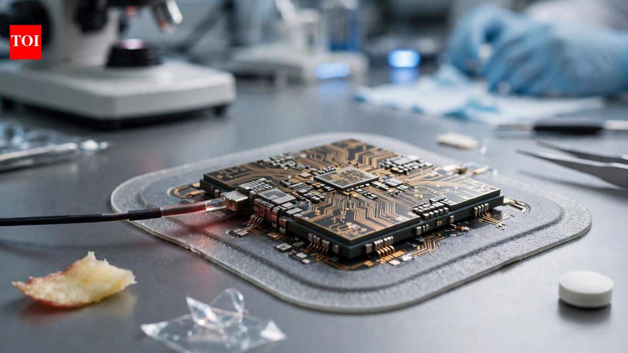
CAMBRIDGE, England — Optical engineers at the University of Cambridge, working in collaboration with the university spin-out venture GlitterinTech, have developed a miniaturized spectrometer chip capable of matching laboratory-grade analytical accuracy at an estimated production cost of approximately $10. The advance, disclosed in findings reported by the TOI Science Desk, shrinks an optical analytical architecture that traditionally requires bulky, fragile benchtop hardware into a sub-centimeter semiconductor format. By drastically lowering the cost and dimensional barriers of optical absorption and reflection profiling, the development clears a technical pathway toward integrating continuous chemical sensing into standard consumer electronics, wearable diagnostic patches, food safety scanners, and industrial sorting systems.
Key facts
What happened
Spectroscopy is an essential tool across chemical analysis, physics, and biological research. The technique works by projecting electromagnetic radiation across a target sample and measuring which wavelengths are absorbed, transmitted, or scattered, revealing an unambiguous chemical fingerprint. For decades, achieving high resolution and wide dynamic range required long optical path lengths, carefully calibrated diffraction gratings, precision collimating mirrors, and sensitive photodetector arrays. These requirements confined reliable spectroscopy primarily to academic and commercial analytical laboratories.
According to reporting by the TOI Science Desk, the research team from the University of Cambridge managed to compress these optical functions onto an integrated micro-scale footprint without degrading measurement fidelity. Partnering with GlitterinTech, an enterprise spun out of the university’s research ecosystem, the engineers engineered an architecture capable of producing reliable spectral data while holding manufacturing costs to roughly $10.
Laboratory tests demonstrated the micro-spectrometer’s ability to discern distinct material types across complex testing matrices. The sensor successfully differentiated between polymer resins commonly found in municipal waste streams, analyzed food compositions for freshness and adulteration, and verified the chemical signatures of finished pharmaceutical formulations. Crucially, the platform showed sufficient sensitivity and stability to support biomedical diagnostic profiling, including non-invasive transdermal tracking of physiological biomarkers.
Why it matters
Lowering the cost of laboratory-grade optical instrumentation from several thousand dollars to the price of a standard microchip represents a structural pivot point for decentralized diagnostics and material quality control. In global health and clinical medicine, diagnostics have frequently been constrained by the logistical bottleneck of central laboratory processing. Blood panels, biomarker evaluations, and drug quality audits often demand days of transit and specialized technician hours. A reliable $10 spectrometer changes that economic calculus. It allows decentralized point-of-care clinics, rural dispensaries, and home-care settings in low-resource environments to conduct real-time screenings without substantial capital budgets.
Beyond centralized medicine, consumer wearable devices stand to undergo a qualitative evolution. Current consumer smartwatches and fitness trackers are predominantly limited to photoplethysmography (PPG), an optical technique using basic green, red, or infrared light-emitting diodes to track heart rate and estimate arterial oxygen saturation by measuring pulse-driven tissue volume changes. Such devices cannot identify specific metabolic chemical compounds. Integrating an actual high-resolution spectrometer on a $10 chip provides the optical bandwidth necessary to track molecular biomarkers through the skin, such as blood glucose trends, hydration indices, lactate accumulation, and alcohol presence, without piercing the skin barrier.
In supply chain logistics, agriculture, and waste management, ubiquitous spectrometry could address critical regulatory failures. The global plastic recycling sector struggles with sorting contamination; automated sorting centers frequently fail to separate chemically incompatible resins like polyethylene terephthalate (PET) and polyvinyl chloride (PVC) at high speeds. Portable handheld scanners running on low-cost chips could allow scrap processors and field inspectors to instantly classify plastics. Similarly, counterfeit and sub-potent pharmaceutical products constitute an estimated multi-billion-dollar threat to public health across emerging markets. Field officers equipped with smartphone-coupled optical wands could authenticate medication packages and blister packs at border checkpoints or pharmacy shelves before dispensing them to patients.
The background
Spectroscopic instruments date back to the 19th-century discoveries of Joseph von Fraunhofer and Gustav Kirchhoff, who demonstrated that atomic elements emit and absorb distinct frequencies of light. Over the following century, the technology bifurcated into several distinct modalities, including ultraviolet-visible (UV-Vis) absorption, near-infrared (NIR), mid-infrared (MIR), and Raman spectroscopy. NIR spectroscopy, in particular, became the workhorse of industrial inspection, agriculture, and pharmaceutical manufacturing because near-infrared light passes partially through organic tissues and packaging materials, exciting molecular vibrational overtones without destroying the sample.
However, conventional NIR and visible-light spectrometers relied on traditional bulk optics. Light entering an optical slit would travel across an internal cavity, bounce off a concave collimating mirror, strike a mechanical or ruled diffraction grating to separate wavelengths, and focus onto an array of charge-coupled devices (CCD) or indium gallium arsenide (InGaAs) photodetectors. Because optical resolution directly scaled with the physical distance the light traveled inside the chamber, miniaturization inevitably caused optical aberrations, cross-talk between wavelengths, and reduced signal-to-noise ratios.
Over the past fifteen years, academic teams worldwide have pursued integrated photonics and computational spectroscopy to bypass physical path-length limits. Approaches have included using dispersive photonic crystal slabs, arrays of quantum dots, micro-electromechanical systems (MEMS) Fabry-Pérot interferometers, and multimode optical fibers paired with machine learning algorithms capable of reconstructing incoming spectra from complex interference speckle patterns. While several semiconductor manufacturers, such as Texas Instruments and ams OSRAM, have brought miniaturized optical sensors to market, units delivering true laboratory-grade spectral selectivity have remained costly—often commanding hundreds to thousands of dollars per unit—or have suffered from narrow spectral bandwidths and high thermal drift.
The University of Cambridge has long maintained specialized expertise in nanofabrication, microelectronics, and advanced photonics, hosted across departments including the Cavendish Laboratory and the Department of Engineering. Spin-outs emerging from the Cambridge technology cluster, commonly termed the Cambridge Phenomenon, have historically served as the primary mechanism for translating university patent portfolios into commercial semiconductor and optoelectronic solutions.
Reaction
The research summary from the TOI Science Desk did not document external third-party reactions or peer commentary following the disclosure. In typical technology transfer cycles of this nature, independent optical physicists, medical device manufacturers, and industrial metrology consortia will evaluate the findings once comprehensive technical white papers and peer-reviewed performance data are made public.
Industry analysts and supply chain observers are anticipated to focus specifically on the claims of laboratory-grade precision at an ultra-low unit cost. While academic prototypes often achieve compelling benchmarks under strictly controlled cleanroom conditions, industrial integration partners will seek verification regarding how the chip tolerates extreme ambient temperature shifts, mechanical shock, optical fouling, and batch-to-batch production variance before committing to integration across mass-market smartphones, consumer electronics, or clinical instrumentation lines.
What we don't know yet
Several fundamental technical parameters remain unverified in the initial disclosure. The reporting by the TOI Science Desk does not specify the precise operational wavelength spectrum of the Cambridge-GlitterinTech chip—namely, whether it operates strictly within the visible spectrum (400–700 nanometers), near-infrared (700–1100 nanometers), or extended short-wave infrared (SWIR, up to 2500 nanometers). This distinction is critical: identifying distinct plastics, hydrocarbons, and pharmaceutical excipients typically demands SWIR coverage, a spectral domain that conventionally requires expensive InGaAs substrates rather than cheap silicon-based fabrication.
Furthermore, the exact resolution metrics, measured in full width at half maximum (FWHM), remain unspecified, as does the device's optical throughput and signal-to-noise ratio in ambient, unshielded outdoor environments. It is also unclear whether the $10 cost estimate represents marginal fabrication costs at wafer scale under high-volume commercial production runs, or the current bill-of-materials cost for low-volume research prototypes, which would exclude packaging, calibration, and integrated illumination light sources.
What to watch
The trajectory of the Cambridge-developed chip will depend on several near-term technical milestones. The primary development to track will be the formal publication of the underlying peer-reviewed study, which will detail the physical architecture, whether it relies on metasurfaces, filter arrays, or computational reconstruction algorithms, and its quantitative limits of detection.
Second, industry observers should monitor regulatory filings and pilot deployments by GlitterinTech. Commercialization pathways will likely involve licensing agreements with established original equipment manufacturers (OEMs) in consumer electronics or automotive sensing. If the startup pursues medical wearable integration, the device will eventually face formal scrutiny from regulatory bodies such as the U.S. Food and Drug Administration (FDA) and the European Medicines Agency (EMA), requiring rigorous clinical trials to prove that transdermal spectral readings correlate accurately with clinical blood-chemistry reference standards under variable human skin tones, hydration levels, and movement.
This report is based on reporting by the TOI Science Desk.
How this story was produced
This report was written by The Global Wire newsroom from reporting first published by TOI Science Desk. We verify the core facts against the original report, write our own account, and add the background and consequences a short wire item leaves out. Drafting is AI-assisted inside an editor-supervised pipeline, and every story is checked for accuracy of attribution, structure and duplication before it appears — full detail in our AI and funding disclosure.
Spotted an error? Tell us at corrections@horizonglobalnews.com and read our corrections policy or editorial standards.






Reader comments
Loading comments…