
Aerosol Jet Printing Advances Enable Circuit Fabrication on 3D Curved Surfaces
A new mist-based printing process allows conductive electronic circuits to be built directly onto complex three-dimensional surfaces, offering new possibilities for structural electronics.
By The Global Wire Newsroom · Reported from Neetika Walter
Link preview · horizonglobalnews.com
Aerosol Jet Printing Advances Enable Circuit Fabrication on 3D Curved Surfaces
A new mist-based printing process allows conductive electronic circuits to be built directly onto complex three-dimensional surfaces, offering new possibilities for structural electronics.
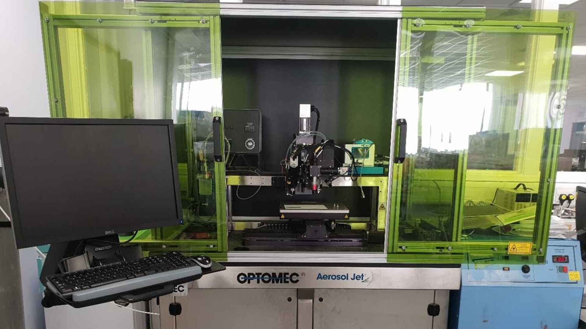
A novel aerosol jet printing technique capable of fabricating high-precision electronic circuitry directly onto complex, curved three-dimensional surfaces has emerged as a potential catalyst for next-generation hardware manufacturing, according to reporting published on September 18, 2026, by technology journalist Neetika Walter. The mist-based deposition method bypasses traditional planar manufacturing constraints by atomizing conductive inks into an ultra-fine aerosol stream, enabling micro-scale trace deposition across irregular contours, spherical shapes, and stepped geometries. By eliminating the requirement for flat circuit board substrates, the technique offers a pathway toward seamlessly integrating sensors, antennas, and interconnects into structural components across aerospace, medical device, and consumer electronics industries.
Key facts
What happened
The development reported by Neetika Walter highlights aerosol jet printing as a non-contact, additive manufacturing technique designed to address the physical limitations of conventional circuit fabrication. In standard electronic manufacturing, conductive pathways are etched onto flat, rigid fiberglass boards—such as standard FR-4 laminates—or flexible polymer sheets using multi-step photolithography, chemical etching, or direct screen printing. These processes fundamentally require planar geometry, forcing design engineers to house flat circuit assemblies within rigid enclosures and connect them via bulky wire harnesses or flexible flat cables.
The mist-based printing method alters this paradigm by converting liquid functional materials—typically ink formulations loaded with conductive metallic nanoparticles, carbon nanomaterials, or functional polymers—into an atomized aerosol cloud. Ultrasonic or pneumatic atomizers break down the liquid ink into microscopic droplets, typically ranging from one to five micrometers in diameter. A dense mist of these droplets is then transported via a carrier gas into a specialized deposition head. Inside the print nozzle, an annular sheath gas flow surrounds the aerosol stream, aerodynamically focusing it into a tightly constrained micro-jet.
Because the focused aerosol stream exits the nozzle as a collimated beam, it maintains high spatial resolution over a standoff distance of several millimeters. This non-contact clearance allows the nozzle to follow the contours of complex, three-dimensional objects without making physical contact with the substrate. Multi-axis motion control systems, such as five-axis robotic gantries or articulating robotic arms, move the print head or target object dynamically, allowing conductive lines, sensor arrays, and interconnects to be printed around tight curves, inside recessed cavities, and across compound non-planar angles. Once deposited, the printed aerosol traces undergo thermal, laser, or photonic sintering to evaporate solvent carriers and fuse the metallic nanoparticles into continuous, highly conductive electrical traces.
Why it matters
The ability to print electronic circuits directly onto three-dimensional, non-planar surfaces represents a structural shift in hardware engineering and product design. In traditional manufacturing, internal space within electronic hardware is heavily constrained by the rectangular geometry of printed circuit boards. By shifting from planar circuit boards to integrated structural electronics, manufacturers can convert the outer shell or structural frame of an object into the circuit board itself.
In aerospace and defense applications, where every gram of weight directly impacts fuel consumption and payload capability, replacing conventional wiring harnesses and bulky circuit boards with direct-write aerosol circuits can reduce total system weight by measurable margins. Curved radar arrays, conformal antennas, and structural health monitoring sensors can be printed directly onto turbine components, wing edges, or fuselage panels, preserving aerodynamic profiles while adding diagnostic capabilities.
In the biomedical sector, mist-based printing opens pathways for customized medical implants and non-invasive wearable monitoring devices. Microscopic sensor networks printed onto the curved surfaces of orthopedic implants, cardiac devices, or dental prostheses could provide real-time telemetry on structural integrity, strain, or biological markers without altering device ergonomics. Furthermore, in consumer electronics and Internet of Things hardware, direct-write mist printing facilitates aggressive miniaturization, allowing smart watches, hearables, and optical devices to incorporate antennas and touch sensors directly onto their curved glass or plastic enclosures, freeing internal volume for larger battery cells or additional processing hardware.
The background
To contextually evaluate the aerosol jet printing advancement reported by Neetika Walter, it is necessary to examine the evolution of printed electronics over the past several decades. Traditional microelectronics relies primarily on photolithography, a subtractive process established in the mid-20th century where silicon wafers or copper-clad laminates are coated with photoresist, exposed to ultraviolet light through photomasks, and chemically etched. While photolithography achieves sub-micron trace resolutions critical for integrated circuits, it requires expensive cleanroom environments, generates substantial chemical waste, and remains strictly limited to flat, planar substrates.
In the late 1990s and early 2000s, additive printed electronics emerged as a lower-cost, high-throughput alternative. Technologies such as screen printing, gravure printing, and drop-on-demand inkjet printing allowed functional inks—such as silver flake suspensions and conductive polymers like PEDOT:PSS—to be applied selectively without subtractive etching. Inkjet printing achieved popularity due to its digital, maskless nature, but it suffers from physical constraints: ink viscosity must be kept within a narrow range (typically 1 to 20 centipoise), nozzle clogging is frequent, and liquid droplets splatter or run when applied to vertical or curved surfaces due to gravity and surface tension.
Aerosol Jet Printing technology was originally developed in the early 2000s, spearheaded by the Defense Advanced Research Projects Agency (DARPA) under its Mesoscopic Integrated Conformal Electronics initiative and commercialized by firms such as Optomec. Unlike inkjet heads that drop macro-droplets directly from orifice plates, aerosol systems separate atomization from deposition. This decoupling allows aerosol jet systems to handle a wider viscosity range—from water-like liquids up to 1,000 centipoise—and utilize higher particle concentrations. Over the past decade, researchers have focused on solving the multi-axis toolpath generation and ink drying physics required to print onto steep vertical walls and complex compound curves without sag or distortion. Advances in functional ink chemistry, including organometallic decomposition inks and low-temperature nanoparticle sintering, have further expanded the range of compatible substrate materials to include temperature-sensitive thermoplastics, elastomers, and biological tissues.
Reaction
While immediate public statements from industry trade groups were not included in the original report by Neetika Walter, semiconductor manufacturing analysts, industrial robotics developers, and biomedical engineers are closely watching the practical deployment of aerosol jet deposition on curved substrates. Equipment manufacturers specializing in additive manufacturing and micro-dispensing are expected to evaluate how mist printing toolpaths can be integrated into existing computer-aided manufacturing software suites, which historically have been optimized for flat planar slicing rather than five-axis conformal toolpaths.
In academic and industrial research labs, material scientists are anticipated to focus on validating the mechanical adhesion of aerosol-printed traces under physical strain, thermal cycling, and environmental exposure. Electronics assembly standards organizations, such as IPC (Association Connecting Electronics Industries), may eventually face demand from tier-one aerospace and automotive suppliers to draft testing protocols specifically tailored for structural electronics printed on non-planar surfaces, where conventional surface-mount technology inspection tools cannot operate.
What we don't know yet
Despite the capabilities outlined in Neetika Walter's report, several critical technical parameters and economic factors remain unverified in the public domain. The reporting does not specify the maximum deposition speed, minimum achievable trace width, or volumetric throughput of this specific mist-based printing implementation, all of which dictate whether the process can transition from low-volume prototyping to mass production lines.
Furthermore, details regarding long-term reliability remain open questions. It is currently unknown how aerosol-printed conductive traces on curved surfaces perform under repeated mechanical flexing, extreme thermal expansion, or moisture exposure compared to standard copper traces on FR-4 circuit boards. The specific thermal sintering requirements—whether the deposited ink requires oven baking at temperatures above 150 degrees Celsius or can be sintered using low-temperature laser or intense pulsed light—will also dictate which substrate plastics or flexible materials can be utilized without causing thermal damage.
What to watch
In assessing the future trajectory of mist-based 3D printed electronics, several specific milestones and technical developments will serve as indicators of commercial viability. Observers should track whether major Electronic Design Automation and Computer-Aided Manufacturing software vendors release native five-axis conformal routing tools designed specifically for aerosol deposition onto complex CAD geometries.
Additionally, industry watchers should monitor corporate announcements from major electronics contract manufacturers and aerospace tier-one suppliers regarding pilot production line integrations. Key indicators of progress will include the publication of peer-reviewed reliability studies examining trace adhesion on curved thermoplastics, the introduction of automated inline optical inspection systems designed for non-planar electronics, and potential standardization efforts by international bodies like IPC to certify 3D printed structural interconnects for high-reliability applications.
This news report is based on original reporting published by technology journalist Neetika Walter on September 18, 2026.
How this story was produced
This report was written by The Global Wire newsroom from reporting first published by Neetika Walter. We verify the core facts against the original report, write our own account, and add the background and consequences a short wire item leaves out. Drafting is AI-assisted inside an editor-supervised pipeline, and every story is checked for accuracy of attribution, structure and duplication before it appears — full detail in our AI and funding disclosure.
Spotted an error? Tell us at corrections@horizonglobalnews.com and read our corrections policy or editorial standards.






Reader comments
Loading comments…