
Northrop Grumman Unveils Rice-Sized FORTITUDE Multilayer GaN Microchip
The FORTITUDE chip uses stacked Gallium Nitride layers to deliver three times more power and 20-fold better signal quality for defense radar and communications.
By The Global Wire Newsroom · Reported from Aamir Khollam
Link preview · horizonglobalnews.com
Northrop Grumman Unveils Rice-Sized FORTITUDE Multilayer GaN Microchip
The FORTITUDE chip uses stacked Gallium Nitride layers to deliver three times more power and 20-fold better signal quality for defense radar and communications.
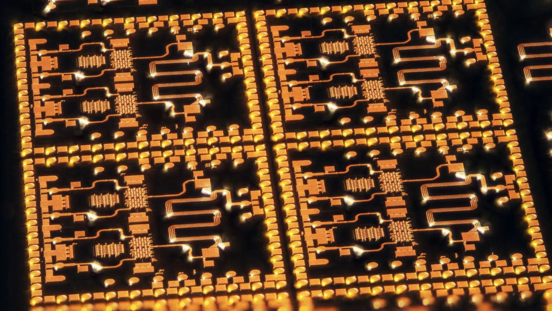
Defense contractor Northrop Grumman has unveiled a new microchip architecture known as FORTITUDE, utilizing a multilayer Gallium Nitride design that achieves a threefold increase in power output alongside a twentyfold improvement in signal quality while remaining roughly the size of a single grain of rice. The development, reported by tech analyst Aamir Khollam on Oct. 2, 2026, represents a notable advancement in semiconductor engineering for radio frequency and defense electronics applications. By stacking Gallium Nitride layers within a miniaturized physical footprint, the design addresses long-standing mechanical and electrical trade-offs between component size, thermal dissipation, and signal clarity in demanding high-frequency environments.
Key facts
What happened
Northrop Grumman disclosed the initial technical performance parameters for its FORTITUDE microchip, marking a new milestone in compound semiconductor design. According to reporting by Aamir Khollam, the defense contractor successfully implemented a multilayer Gallium Nitride (GaN) layout on a chip die engineered down to the scale of a rice grain.
Traditional radio frequency (RF) integrated circuits typically rely on single-layer planar semiconductor layouts. In conventional designs, increasing the transmission power requires expanding the lateral surface area of the chip or increasing the current running through planar conductive traces. However, pushing higher electrical power through planar structures rapidly creates severe heat accumulation, resistive power losses, and electromagnetic cross-talk that distorts signal fidelity.
To bypass these physical constraints, Northrop Grumman constructed FORTITUDE using a 3D multilayer architectural topology. By stacking functional GaN semiconductor layers vertically, the chip drastically reduces the physical length of internal conductive paths. This shortened interconnect structure minimizes parasitic capacitance and resistive losses while maintaining tight signal paths. The technical result reported by Khollam is a device capable of outputting three times more RF power while simultaneously reducing noise and harmonic distortion to deliver a 20-fold gain in overall signal quality.
The miniaturized size of the FORTITUDE chip allows it to be integrated into space-constrained hardware assemblies. Modern electronic warfare pods, active electronically scanned array (AESA) radar modules, and tactical software-defined radios require front-end RF chips that can handle elevated power levels without compromising thermal stability or occupying critical internal volume. Northrop Grumman's design leverages the fundamental physical properties of GaN—notably its high electrical breakdown field and rapid electron mobility—to sustain these performance levels within a millimeter-scale die.
Why it matters
The operational capabilities reported for the FORTITUDE chip carry significant implications for Size, Weight, and Power (SWaP) optimization across military, aerospace, and high-performance wireless applications. In modern defense electronics, physical space and available electrical energy are primary operational constraints. Achieving a threefold increase in output power within a rice-sized package directly alters baseline system engineering calculations.
A 3x increase in power output enables RF transmitters to extend their operational range, penetrate dense atmospheric obstruction, or burn through high-power enemy jamming signals without requiring larger external electrical generators or expanded liquid cooling infrastructure. On platforms with strict weight and volume limits—such as uncrewed aerial vehicles (UAVs), satellite constellations, guided munitions, and tactical aircraft—the ability to replace larger RF assemblies with a single microchip frees up internal volume for fuel, secondary sensors, or additional physical payload.
Simultaneously, the 20-fold boost in signal quality directly improves sensor sensitivity and secure communication link budgets. Higher signal purity allows RF receivers to extract faint data streams from noisy electromagnetic environments. In electronic warfare scenarios, a cleaner signal reduces self-interference, allowing friendly forces to jam enemy communications or radar channels without disrupting their own radio links. For radar systems, superior signal clarity improves target discrimination, enabling defense systems to detect smaller radar-cross-section targets, such as stealth aircraft or micro-drones, at greater stand-off ranges.
Beyond defense applications, advances in multilayer GaN fabrication establish important technical benchmarks for commercial telecommunications. As high-capacity wireless infrastructure pushes toward millimeter-wave frequencies—including advanced 6G networks and dense low-Earth-orbit satellite broadband arrays—the demand for highly efficient, compact RF power amplifiers with minimal signal distortion is increasingly aligned with defense requirements.
The background
The adoption of Gallium Nitride in microelectronics represents the latest stage in a decades-long evolution of semiconductor materials for high-frequency power electronics. For decades, silicon (Si) formed the foundation of solid-state electronics. However, silicon's narrow bandgap energy of approximately 1.1 electron volts imposes strict physical limits on maximum operating voltage, thermal resistance, and switching speeds.
During the 1980s and 1990s, the defense and telecommunications sectors increasingly turned to Gallium Arsenide (GaAs) for high-frequency microwave applications. While GaAs offered superior electron mobility compared to silicon, it lacked high voltage handling and thermal conductivity, restricting its effectiveness in high-power radar and transmitter systems.
The emergence of Gallium Nitride in the early 2000s marked a major technological shift. As a wide-bandgap material with an energy bandgap of approximately 3.4 electron volts, GaN exhibits a critical electric breakdown field nearly ten times greater than that of silicon, alongside significantly higher thermal conductivity. These material properties permit GaN transistors to operate at much higher supply voltages, higher temperatures, and elevated frequencies without experiencing breakdown. The U.S. Defense Advanced Research Projects Agency (DARPA) and service research laboratories invested heavily in GaN manufacturing capabilities over the past two decades to support modern military radars and electronic warfare systems.
Northrop Grumman maintains extensive internal microelectronics research and fabrication facilities, producing specialized compound semiconductors for major defense programs. The company has integrated GaN microelectronics into systems such as air-to-air radars, missile defense sensors, and satellite communications payloads.
As basic GaN fabrication has matured across the semiconductor industry, research has turned toward advanced 3D packaging and multilayer integration. Traditional planar GaN designs reached physical boundaries regarding layout density and thermal spreading. Constructing multilayer GaN devices requires solving complex material engineering challenges, including thermal expansion matching between stacked layers, precise vertical interconnect fabrication, and effective heat extraction from embedded internal junctions. The FORTITUDE chip reflects this transition from single-layer planar devices to complex 3D semiconductor architectures.
Reaction
Official statements from U.S. defense procurement offices, military branches, or industry competitors regarding the FORTITUDE release have not yet been made public following the initial report by Aamir Khollam.
Industry analysts expect the technical metrics of the FORTITUDE chip to draw close scrutiny from government microelectronics initiatives, such as the U.S. Department of Defense's Microelectronics Commons and DARPA's Microsystems Technology Office. These organizations track advances in compound semiconductors to assess national defense industrial base capabilities and supply chain resilience.
Major aerospace and defense prime contractors competing in the radio frequency and electronic warfare markets—including Raytheon, Lockheed Martin, and L3Harris Technologies—will likely monitor the development to evaluate how multilayer GaN topology affects competing RF payload offerings. Defense procurement officials will also watch whether Northrop Grumman intends to use FORTITUDE exclusively within its own proprietary systems or make the semiconductor technology available to third-party defense integrators.
What we don't know yet
While the preliminary metrics released for the FORTITUDE chip demonstrate substantial performance gains, several key technical and manufacturing details remain unconfirmed in available reports:
What to watch
Over the coming months, several key milestones will clarify the operational status and broader impact of Northrop Grumman's FORTITUDE chip:
This report is based on coverage originally published by tech reporter Aamir Khollam.
How this story was produced
This report was written by The Global Wire newsroom from reporting first published by Aamir Khollam. We verify the core facts against the original report, write our own account, and add the background and consequences a short wire item leaves out. Drafting is AI-assisted inside an editor-supervised pipeline, and every story is checked for accuracy of attribution, structure and duplication before it appears — full detail in our AI and funding disclosure.
Spotted an error? Tell us at corrections@horizonglobalnews.com and read our corrections policy or editorial standards.



Reader comments
Loading comments…