

Micron Commits $10 Billion for Advanced Memory and Chip Packaging Laboratory in Boise
The $10 billion research facility in Idaho aims to pioneer post-silicon memory architectures, advanced packaging, and next-generation compute technologies.
By The Global Wire Newsroom · Reported from Neetika Walter
Link preview · horizonglobalnews.com
Micron Commits $10 Billion for Advanced Memory and Chip Packaging Laboratory in Boise
The $10 billion research facility in Idaho aims to pioneer post-silicon memory architectures, advanced packaging, and next-generation compute technologies.
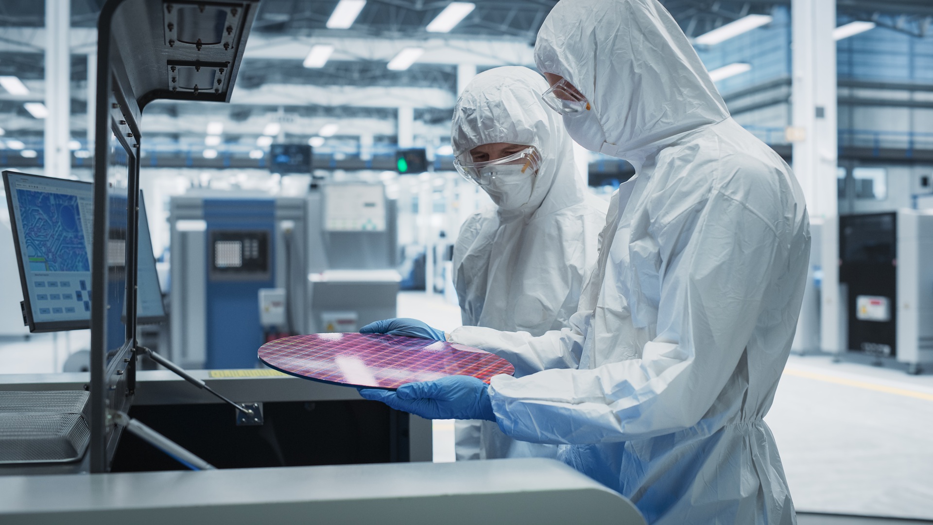
Micron Technology has committed $10 billion to build a research and development laboratory in Boise, Idaho, dedicated to developing next-generation memory architectures, advanced chip packaging, and novel computing designs. According to reporting by Neetika Walter, the planned facility will focus on memory technologies that go beyond current industry standards, aiming to solve critical processing and bandwidth limits in artificial intelligence and supercomputing. The commitment represents one of the largest single research site investments in the history of the American semiconductor industry and reinforces Boise as Micron's core global technological hub.
Key facts
What happened
Micron’s $10 billion commitment allocates dedicated capital toward building a specialized laboratory environment capable of prototyping technologies far beyond today's leading-edge manufacturing nodes. The initiative targets four main technical disciplines: next-generation memory design, advanced packaging, revolutionary computing paradigms, and novel semiconductor fabrication techniques, as reported by Neetika Walter.
In conventional microelectronics, hardware scaling relies on shrinking transistors on a two-dimensional plane. However, as silicon lithography approaches atomic boundaries, physical limitations such as electrical leakage, excessive thermal output, and parasitic capacitance make conventional miniaturization increasingly difficult and expensive. Micron’s new Boise laboratory is structured to focus on post-silicon and non-volatile memory research, exploring material science innovations and three-dimensional chip design.
Key focus areas for the laboratory include:
By uniting these disciplines within a single research facility, Micron intends to accelerate the transition of laboratory breakthroughs into high-volume commercial manufacturing lines.
Why it matters
The technological priorities targeted by Micron's new laboratory lie at the exact intersection of the most severe bottlenecks facing modern artificial intelligence and data center operations. Over the past decade, processor speed and compute density have expanded at a far faster rate than memory bandwidth and capacity—a disparity known in the technology industry as the "memory wall."
Large language models, deep learning neural networks, and high-performance computing clusters require massive quantities of data to be streamed into processing units simultaneously. When processor cores are forced to wait for memory buses to deliver data, chip performance stalls and energy usage spikes. High-Bandwidth Memory (HBM)—which stacks multiple DRAM dies vertically using Through-Silicon Vias (TSVs)—has emerged as a vital bridge, but present-day HBM designs face thermal and manufacturing yields constraints. Micron's focus on next-generation packaging and architectures is designed to remove these performance ceilings.
Economically, the $10 billion commitment solidifies the position of the United States in foundational semiconductor research. While chip fabrication facilities (fabs) produce mature commercial wafers, R&D laboratories create the proprietary intellectual property, material patents, and process recipes that dictate long-term market leadership. Micron competes directly with South Korea's Samsung Electronics and SK Hynix in the global memory sector, which accounts for roughly 25 to 30 percent of the total semiconductor market. SK Hynix currently holds a strong position in HBM memory supplied to AI hardware developers like Nvidia, making Micron's aggressive R&D investment a strategic necessity to secure future market share in AI memory supply chains.
The background
Founded in 1978 in a Boise dental office basement, Micron Technology has grown into the primary United States-headquartered manufacturer of memory chips. Over four decades, the company built its enterprise on standard DRAM—used for volatile, high-speed system memory—and NAND flash, used for non-volatile storage in solid-state drives (SSDs) and mobile devices.
However, memory manufacturing has historically been subject to extreme capital cycles, characterized by severe price swings, capacity oversupply, and high capital expenditure requirements. To protect profitability and retain technical parity with international competitors, memory makers have been forced to continually innovate on yield efficiency and circuit density.
The global landscape shifted dramatically following the passage of the U.S. CHIPS and Science Act of 2022, a federal law granting $52.7 billion in direct subsidies, loan guarantees, and tax credits to incentivize domestic semiconductor manufacturing and research. Following the law's enactment, Micron outlined multi-decade, tens-of-billions-of-dollars expansion plans within the United States, including major fabrication complexes in Clay, New York, and a co-located leading-edge memory fab in Boise, Idaho.
While commercial fabs execute high-volume manufacturing of current-generation process nodes, the newly announced $10 billion laboratory operates further upstream in the technology life cycle. It serves as an incubator for physical concepts that will not reach commercial fabrication lines for five to ten years. Idaho has historically served as Micron's primary research hub; even as the company expanded volume production to Singapore, Japan, and Taiwan, initial process technology recipes and pilot line developments consistently originated at its Boise headquarters.
Reaction
While formal public statements from executive officers and state officials were not detailed in the original reporting, major capital investments of this magnitude typically prompt structured responses across state, federal, and industry platforms.
State and local government leadership in Idaho are expected to endorse the project, as large-scale semiconductor research investments generate thousands of secondary specialized engineering, construction, and facility maintenance jobs while expanding the local tax base. Federal economic officials, particularly within the U.S. Department of Commerce, are likely to point to the facility as concrete evidence that domestic semiconductor legislation is successfully drawing foundational microelectronics innovation back to American soil.
Industry analysts and hardware engineers view the announcement as a clear signal that the semiconductor industry is shifting its focus away from purely shrinking transistors and toward radical architectural shifts. Wall Street equity analysts will monitor Micron's capital expenditure guidance to assess how the $10 billion investment will be amortized across multi-year research budgets, balancing immediate corporate margin goals against long-term competitive positioning.
What we don't know yet
Despite the scale of the $10 billion announcement, several key operational details remain unconfirmed:
What to watch
In the coming months, several key development points will clarify the scope and progress of the Boise facility:
This account is based on reporting by Neetika Walter.
How this story was produced
This report was written by The Global Wire newsroom from reporting first published by Neetika Walter. We verify the core facts against the original report, write our own account, and add the background and consequences a short wire item leaves out. Drafting is AI-assisted inside an editor-supervised pipeline, and every story is checked for accuracy of attribution, structure and duplication before it appears — full detail in our AI and funding disclosure.
Spotted an error? Tell us at corrections@horizonglobalnews.com and read our corrections policy or editorial standards.

Reader comments
Loading comments…