

IBM Unveils 2nm Enterprise Processor Unifying Arm and Mainframe Architectures
IBM has detailed an 11-core, 2-nanometre processor operating above 5.7 GHz that integrates Arm compute cores with traditional mainframe architecture on single silicon.
By The Global Wire Newsroom · Reported from Neetika Walter
Link preview · horizonglobalnews.com
IBM Unveils 2nm Enterprise Processor Unifying Arm and Mainframe Architectures
IBM has detailed an 11-core, 2-nanometre processor operating above 5.7 GHz that integrates Arm compute cores with traditional mainframe architecture on single silicon.
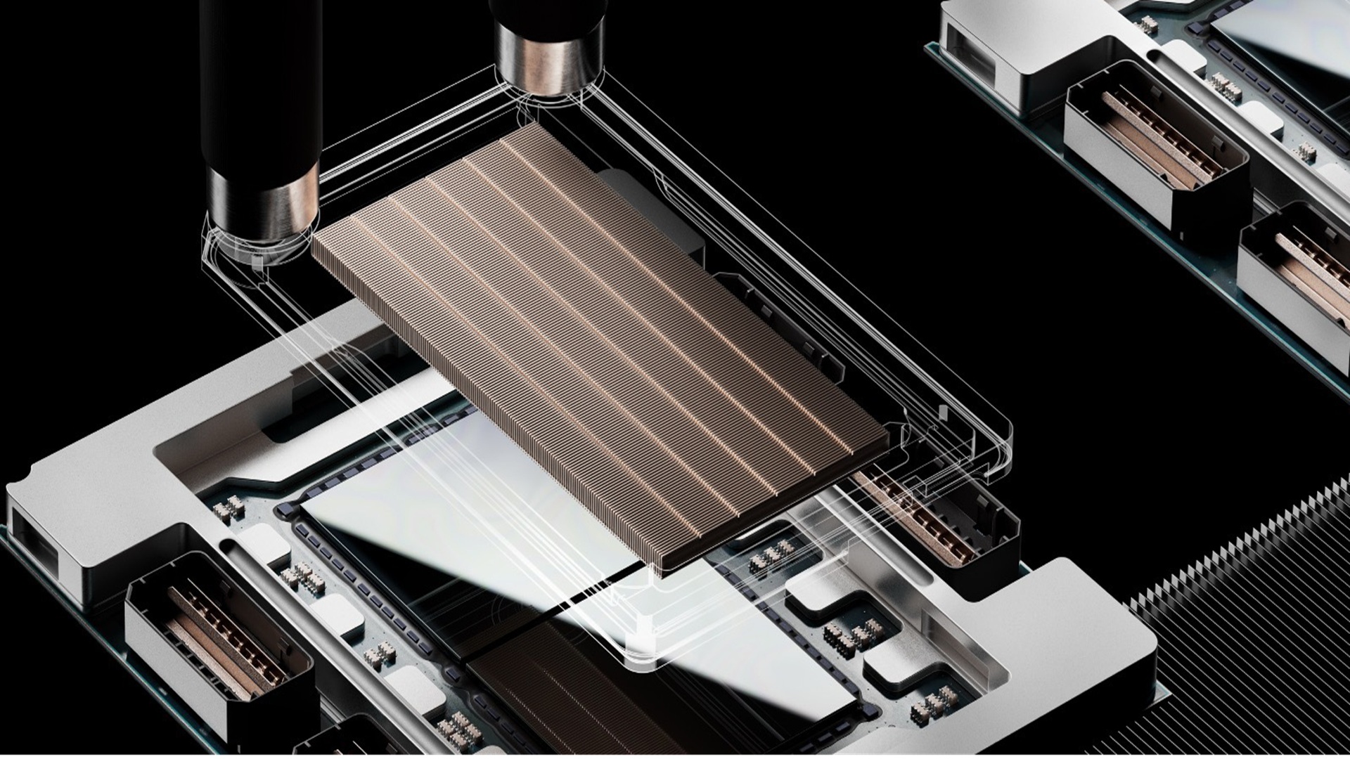
International Business Machines Corp. has unveiled a 2-nanometre processor engineered for dual-architecture enterprise workloads, integrating Arm processor cores alongside traditional mainframe compute units on a single piece of silicon. According to reporting by Neetika Walter, the new chip achieves operational clock frequencies exceeding 5.7 gigahertz and incorporates an 11-core layout designed to bridge the gap between lightweight, highly efficient reduced instruction set computer (RISC) workloads and heavy enterprise transaction processing. The announcement represents a major structural shift in enterprise silicon design, combining IBM's proprietary mainframe instruction sets with mainstream Arm execution units to target hybrid cloud datacenters and modern transaction processing environments.
Key facts
What happened
IBM revealed a 2-nanometre silicon processor designed to unify Arm computing capabilities and enterprise mainframe processing within a single physical chip, as reported by Neetika Walter. Developed to address complex datacenter environments, the processor features 11 cores capable of running at clock speeds top-ending above 5.7 gigahertz.
The technical design targets dual-architecture execution, allowing high-frequency, heavy-throughput transaction processing to run side-by-side with modern microservices built on the Arm instruction set architecture. Rather than relying on separate physical server blades, distinct compute clusters, or software emulation layers to connect mainframe databases with containerized cloud applications, the chip integrates both computational instruction sets directly into the same piece of 2-nanometre silicon.
The layout seeks to deliver the continuous processing reliability, rapid single-thread clock speeds, and extreme memory bandwidth associated with enterprise mainframes alongside the energy efficiency and broad software compatibility of the Arm ecosystem. Running at frequencies beyond 5.7 gigahertz positions the 11-core chip among the fastest enterprise processors in active development, continuing IBM's long-standing design focus on high single-thread clock rates for mission-critical enterprise workloads.
Why it matters
The introduction of a dual-architecture 2-nanometre processor operating above 5.7 gigahertz directly addresses structural operational challenges in modern enterprise datacenters. For decades, global financial institutions, insurance providers, healthcare networks, and government agencies have relied on mainframe systems for high-volume, zero-downtime transaction processing. However, modern software development has increasingly standardized on cloud-native containerized applications and microservices optimized for RISC architectures like Arm. By placing mainframe processing units and Arm cores on a single 11-core die, IBM aims to streamline datacenter hardware footprints, enabling organizations to execute legacy transaction code and modern microservices on unified hardware without incurring the network latency or power overhead associated with multi-system communication.
From a microarchitectural perspective, sustaining operational clock speeds beyond 5.7 gigahertz on an advanced 2-nanometre manufacturing node represents a notable engineering milestone. Operating at higher clock frequencies generates significant heat and electrical current density, particularly as transistor features scale down to single-digit nanometres where quantum tunneling and power leakage become severe physical constraints. Managing stable high-frequency execution across an 11-core layout requires sophisticated power distribution networks and advanced thermal management within the chip package.
For enterprise technology managers and datacenter operators, dual-architecture chips offer a pathway to consolidate server racks, manage electricity consumption, and lower thermal cooling costs. As cloud service providers continue to expand custom Arm-based server silicon, IBM's hybrid design provides enterprise clients with a mechanism to modernize software stacks while retaining native hardware execution for core banking and transaction systems.
The background
To understand the context of this development, IBM has historically maintained a unique position in semiconductor research and enterprise computing architecture. While the general-purpose server market came to be dominated by x86 processors manufactured by Intel and AMD, IBM maintained its proprietary z/Architecture mainframes and POWER series chips for specialized enterprise markets that demand high memory bandwidth, non-stop uptime, and deterministic real-time processing.
In May 2021, IBM Research announced the creation of a 2-nanometre test chip at its Albany Nanotech Complex in New York. That experimental design utilized gate-all-around (GAA) nanosheet transistor technology, scaling transistor density to fit up to 50 billion transistors into a chip roughly the size of a fingernail. At the time of that research breakthrough, IBM projected that 2-nanometre process nodes could deliver either a 45 percent performance improvement or a 75 percent reduction in energy consumption compared to the 7-nanometre chips then in mainstream commercial production.
Over the same period, the broader datacenter industry underwent a significant migration toward Arm architecture. Originally designed by Arm Ltd. for mobile devices and low-power mobile applications, RISC-based Arm designs gained widespread adoption in hyperscale cloud facilities due to their power efficiency, scalable core designs, and flexible licensing terms. Major cloud providers developed proprietary Arm server processors to power web-scale infrastructure, placing pressure on legacy enterprise platforms to interact seamlessly with Arm-based cloud software.
IBM's mainframe platform, represented in recent years by systems such as the z15 released in 2019 and the z16 launched in 2022—which featured the 7-nanometre Telum processor operating at 4.6 gigahertz with integrated on-chip artificial intelligence accelerators—relied on specialized execution pipelines tailored for decimal arithmetic, bulk encryption, and heavy input/output operations. Bringing Arm cores directly onto enterprise mainframe silicon represents a strategic evolution to adapt z/Architecture platforms to hybrid cloud infrastructure without requiring customers to perform risky, complete rewrites of legacy mainframe software.
Reaction
While formal public statements from competing chipmakers and server vendors were not detailed in the initial coverage, industry analysts and enterprise infrastructure architects are expected to scrutinize the benchmark performance and practical deployment model of the dual-architecture processor. Observers in the enterprise technology sector anticipate that major financial institutions and government agencies—the primary consumer base for mainframe hardware—will closely examine the processor's thermal profile, backwards software compatibility, and real-world energy consumption.
Competitors in the enterprise processor market, including developers of x86 server chips and designers of custom hyperscale Arm processors, will monitor how IBM's dual-architecture approach impacts total cost of ownership in high-density datacenters. Semiconductor industry analysts are also expected to evaluate the commercial scalability, wafer yields, and production manufacturing partners associated with bringing 2-nanometre enterprise processors to full commercial production.
What we don't know yet
Several key technical specifications and commercial parameters regarding the 2-nanometre dual-architecture processor were omitted from the initial reporting. The specific allocation of the 11 cores—namely how many are dedicated to standard Arm instruction set execution versus proprietary mainframe compute engines—has not been publicly specified. Furthermore, details regarding on-chip cache levels (such as L1, L2, and L3 cache capacities), memory channel architecture, and bus interconnect speeds remain unconfirmed.
The identity of the semiconductor foundry partner manufacturing the 2-nanometre silicon was also not specified in the available report. Because IBM transitioned its commercial fabrication facilities to GlobalFoundries in 2015 and operates primarily as a fabless research and design entity, volume production of 2-nanometre commercial chips relies on external manufacturing foundries such as Samsung Electronics or Taiwan Semiconductor Manufacturing Company (TSMC).
Additionally, commercial availability dates, server chassis configurations, power consumption metrics (such as thermal design power in watts), and pricing models have not yet been released. It remains unconfirmed whether this dual-architecture processor will be integrated exclusively into IBM's full-frame zSystem enterprise servers or made available in standalone modular rack server configurations.
What to watch
In the coming months, technology analysts should look for detailed architectural whitepapers and technical disclosures from IBM outlining the physical floorplan, instruction switching interfaces, and cache coherence mechanisms of the 11-core chip. Independent performance benchmarks comparing real-world transaction throughput and containerized microservice execution against existing enterprise processors will serve as a primary gauge of market competitiveness.
Key milestones to follow include official announcements regarding commercial shipment timelines, system integration options, and enterprise operating system support. Datacenter operators will watch whether major enterprise Linux distributions and container management platforms issue native updates optimized to schedule workloads across both compute architectures on a single die. Finally, updates regarding 2-nanometre manufacturing yield rates and supply chain logistics will determine the speed at which this hybrid architecture can be deployed in enterprise datacenters globally.
This report is based on original news coverage published by Neetika Walter.
How this story was produced
This report was written by The Global Wire newsroom from reporting first published by Neetika Walter. We verify the core facts against the original report, write our own account, and add the background and consequences a short wire item leaves out. Drafting is AI-assisted inside an editor-supervised pipeline, and every story is checked for accuracy of attribution, structure and duplication before it appears — full detail in our AI and funding disclosure.
Spotted an error? Tell us at corrections@horizonglobalnews.com and read our corrections policy or editorial standards.
Reader comments
Loading comments…